40 how to draw energy band diagram
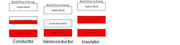
Draw separate energy band diagrams for conductors, semi ... Draw separate energy band diagrams for conductors, semi-conductors and insulators and label each of them. Medium Solution Verified by Toppr Energy band diagrams for conductor, semiconductor and insulator are shown above. In conductors, both the valance band and conduction band overlap each other. So there is zero band gap in a conductor. Draw and explain energy band diagram of MOS capacitor in ... The energy band diagram contains the electron energy levels in the MOS structure as deliniated with the fermi energy in the metal and semiconductor as well as the conduction and valence band edge in the oxide and the silicon.
Semiconductors - Energy bands, types of semiconductors and ... The diagram shows the energy band diagram of pure semiconductor at room temperature, the electrons are present in the valence band as shown. Now at high temperature or by receiving some additional energy the electron from valence band jumps to the conduction band.

How to draw energy band diagram
Multi-Dielectric Energy Band Diagram Program - The ... Draw band diagrams for MOS devices in static mode; Draw band diagrams for MOS and MIM gate stacks with various dielectrics, including high-κ dielectrics; Show band diagram movement for MOS and MIM devices as gate voltage is swept through a range; Calculate these parameters for applied voltages both in inversion and accumulation regimes: energy Draw and explain energy band diagram of MOS capacitor in ... Energy band bending is changes in energy offset (level) of semiconductor's band structure near junction due to space charge. 2. Depletion layer: In depletion region, voltage applied to gate is greater than flat band voltage and less than threshold voltage. Fig2 energy band diagram and MOSFET internal charge distribution in depletion region Band Diagram Calculator | Heterojunction | PN Junction ... Simple PN Junction | Heterojunction Energy Band Diagram Graphical Model and Calculator Based on Microsoft Excel. CREDITS. Salman Bawa. Samuel Peter. Dr. Adrian Kitai. Download Band Diagram Calculator ...
How to draw energy band diagram. Energy Bands - Definition and Classification of Energy ... The energy band diagram of semiconductor is shown where the conduction band is empty and the valence band is completely filled but the forbidden gap between the two bands is very small that is about 1eV. For Germanium, the forbidden gap is 0.72eV and for Silicon, it is 1.1eV. Thus, semiconductor requires small conductivity. Energy Band Theory Draw the energy band diagrams of p-type and n-type ... Zigya App Draw the energy band diagrams of p-type and n-type semiconductors. A semiconductor has equal electron and hole concentration 6 x 10 8 m -3. On doping with a certain impurity, electron concentration increases to 8 x 10 12 m -3. Identify the type of semiconductor after doping. 1301 Views Switch Flag Bookmark Lecture 5.2: Energy band diagrams - nanoHUB Energy band diagrams . Lundstrom: 2018 . An energy band diagram is a plot of the bottom of the conduction band and the top of the valence band vs. position. Energy band diagrams are a powerful tool for understanding semiconductor devices because they provide . qualitative solutions to the semiconductor equations. Is there any software available to draw the energy band ... In Microsoft work. you can easily draw your energy band diagram with few minute. Follow step: open Microsoft Word..go insert window...shapes.. New Drawing canvas. Good luck Cite 1 Recommendation...
Band diagram - Wikipedia The band diagram may be shown connected to a circuit diagram showing how bias voltages are applied, how charges flow, etc. The bands may be colored to indicate filling of energy levels, or sometimes the band gaps will be colored instead. Energy levels Energy Diagrams of PN Junction & Depletion Region - Inst Tools An energy diagram for a pn junction at the instant of formation is shown in Figure (a). As you can see, the valence and conduction bands in the n region are at lower energy levels than those in the p region, but there is a significant amount of overlapping. The free electrons in the n region that occupy the upper part of the conduction band in ... How to draw the energy band diagram for a semiconductor ... A schematic diagram of a silicon-oxide-silicon structure is shown. The top and bottom silicon electrodes are uniformly doped. The top silicon electrode is N-type and its dopant concentration is 2E16 cm-3. The bottom silicon electrode is p-type and its dopant concentration is 1E16cm-3. The oxide layer is 30nm thick and free from defects. Energy Band Diagram BASICS | Shortcuts to draw ANY Energy ... Hey Comrades! If you want to learn THE EASIEST METHOD to draw ANY Energy Band Diagram (EBD), then this video is a must-watch for you. I classified the 2 fact...
Draw separate energy band diagrams for conductors ... Complete step-by-step answer: An energy band is the range of energy of electrons possessed in an atom. According to the energy band theory, the valence band, conduction band and forbidden band determine the conductive properties of materials. Valance band can be defined as the last filled energy band of material at 0K. PDF Energy Band Diagrams - nanoHUB Energy band diagrams Lundstrom: Fall 2019 An energy band diagram is a plot of the bottom of the conduction band and the top of the valence band vs. position. Energy band diagrams are a powerful tool for understanding semiconductor devices because they provide qualitative solutions to the semiconductor equations. 5 Energy band diagrams Energy Band Diagrams | Semiconductor Theory This can be illustrated with an energy band diagram, which shows two energy levels, a valence band and a conduction band. Valence electrons are located in the valence band and the free electrons in the higher conduction band. In semiconductors there is a gap between the valence and conduction bands. Energy Band Diagram - an overview | ScienceDirect Topics Energy-band diagrams beneath the gate in various doped heterostructure FETs. The GaAs-gate SISFET in Fig. 23b is similar to the MISFET, except for the replacement of the metal gate with n+ GaAs. This results in a change in barrier height, which in turn causes a shift in the fixed threshold to -0.1 V (normally on).
Important Questions for CBSE Class 12 Physics Semiconductor, Diode and its Applications
How to Draw and Understand Energy Band Diagram of Pn ... This quick video will give you a complete analysis of energy band diagram of pn juction diode
Solved: The Following Energy Band Diagram Characterizes A ... | Chegg.com
Energy Band Diagram - an overview | ScienceDirect Topics Figure 1 shows the energy band diagram of an electrolyte insulator semiconductor (EIS) structure. When light with more energy than the band gap of Si (1.1 eV) illuminates the back of the Si substrate, electrons in the valence band are excited into the conduction band.
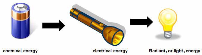
How A Flashlight Works
PDF Overview of Silicon Semiconductor Device Physics Band Diagrams (Revisited) E. g. E. C. E. V. Band Diagram Representation. Energy plotted as a function of position. E. C. ÆConduction band. ÆLowest energy state for a free electron. ÆElectrons in the conduction band means current can flow. E. V. ÆValence band ÆHighest energy state for filled outer shells ÆHoles in the valence band means ...

Photosynthesis Light Reaction Simple Diagram
What is Energy Band : Band Theory and Different Types The following images show the semiconductor's energy band diagram wherever the conduction band can be vacant & the valence band is totally filled however the forbidden gap among these bands is minute that is 1eV. The forbidden gap of Ge is 0.72eV and Si is 1.1eV. Therefore, semiconductor needs little conductivity. energy-band-in-semiconductors
Electrical Conduction Animation
1.09 Energy band diagrams in metals ... - Science Campus 1.09 Energy band diagrams in metals, semiconductors and insulators. In a metal the conduction and valence bands overlap so electrons can easily pass into the conduction band. This means that the number density of free charge carriers will be very high. In semiconductors there is a gap between the valence band and conduction band, also the ...
0 Response to "40 how to draw energy band diagram"
Post a Comment