38 phase lock loop block diagram
rfic.eecs.berkeley.edu › ee242 › pdfPhase Locked Loops (PLL) and Frequency Synthesis simulation. But the dynamics of the loop, such as settling time, the noise transfer characteristics (phase noise), can be derived from a linear model. Therefore it is useful to derive a linear model by assuming the system is close to lock, or in lock. The most convenient variable is phase, and not frequency, in the linear model. › linear_integratedPhase Locked Loop IC - Tutorialspoint Phase Locked Loop (PLL) is one of the vital blocks in linear systems. It is useful in communication systems such as radars, satellites, FMs, etc. This chapter discusses about the block diagram of PLL and IC 565 in detail. Block Diagram of PLL. A Phase Locked Loop (PLL) mainly consists of the following three blocks −. Phase Detector; Active ...
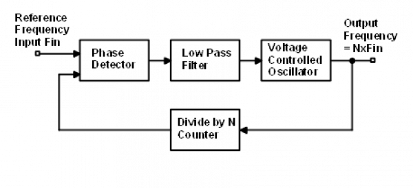
Describe the basic block diagram of the phase locked loop (PLL). Following figure shows the block diagram of PLL. It consists of. Phase detector. Low pass filter. Voltage Controlled Oscillator (VCO) The phase detector compares the input frequency fi with the feedback frequency fo and generates an output signal which is a function of the difference between the phases of the two input signals. The output ...

Phase lock loop block diagram
› ~jph7 › websiteLock - in Amplifier and Applications - Lehigh University frequency, and θsig is the signal’s phase. Lock-in amplifiers generate their own internal reference signal usually by a phase-locked-loop locked to the external reference. In the diagram below the external reference, the lock-in’s reference and the signal are all shown. The internal reference is VLsin(ωot + θref). PDF Phase Locked Loop Circuits - UC Santa Barbara which the loop will lock when starting from an unlocked condition. Sometimes a frequency detector is added to the phase detector to assist in initial acquisition of lock. You will see later that the loop filter bandwidth has an effect on the capture range. 7. Approach: We will discuss the details of phase detectors and loop filters as we proceed. › lit › anCD4046B Phase-Locked Loop: A Versatile Building Block for ... 4 CD4046B Phase-Locked Loop: A Versatile Building Block for Micropower Digital and Analog Applications 3 CD4046B PLL Technical Description Figure 2 shows a block diagram of the CD4046B, which has been implemented on a single monolithic integrated circuit. The PLL structure consists of a low-power, linear VCO and two
Phase lock loop block diagram. Phase Locked Loop Working Principle | PLL block diagram | EEEGUIDE Phase Locked Loop Working Principle: A Phase Locked Loop Working is basically a closed loop system designed to lock the output frequency and phase to the frequency and phase of an input signal. It is commonly abbreviated as Basics of PLL. The PLL was first introduced in its discrete form in early 1930s. Phase Lock Loop - Patel - Google Search Figure 1: Block diagram of a Phase Lock Loop, frequency multiplier circuit. This frequency multiplier circuit is basically a feedback control system that controls the phase of a voltage controlled oscillator (VCO). The input signal is applied to one input of the phase detector. The other input is connected to the output of a divide by N counter. PDF Phase Lock Loop Control System Lab Development The Block Diagram of the Phase Lock Loop An effective way to look at Figure 1 i s to begin with the Voltage Controlled Oscillator (VCO). The VCO converts a dc input (V e(t)) into a sinusoidal signal (V vco (t) with cyclic frequency f (Hz)) at the output . To accomplish a VCO by itself, one can use operational amplifiers if an Phase-locked Loop - Phase-locked Loop Block Diagram Phase-locked Loop Block Diagram. ... A digital phase locked loop uses a digital phase detector; it may also have a divider in the feedback path or in the reference path, or both, in order to make the PLL's output signal frequency a rational multiple of the reference frequency. A non-integer multiple of the reference frequency can also be ...
Predicting the Phase Noise and Jitter of PLL-Based Frequency … The block diagram of a PLL operating as a frequency synthesizer is shown in Figure 1 [8]. It consists of a reference oscillator (OSC), a phase/frequency detector (PFD), a charge pump (CP), a loop filter (LF), a voltage-controlled oscillator (VCO), and two frequency dividers (FDs). The PLL is a feedback loop that, wh en in lock, forces › phase-locked-loop-operatingPhase Locked Loop Operating Principle and Applications The below figure shows the block diagram of the PLL. Phase-Locked Loop Detector. The phase-locked loop detector compares the input frequency and the output frequency of the VCO to produces a DC voltage which is directly proportional to the phase distinction of the two frequencies. The analog and digital signals are used in the phase-locked loop. Phase Locked Loop - an overview | ScienceDirect Topics The block diagram of a phase locked loop. (11.35) f ref = f d = F out N. or (11.36) F out = N f ref. ... Some FPGA clock managers are based on phase-locked loops (PLLs), while others are based on digital delay-locked loops (DLLs). PLLs have been used since the 1940s in analog implementations, but recent emphasis on digital methods has made it ... knowledge.ni.com › KnowledgeArticleDetailsWhat Is a Phase-Locked Loop (PLL)? - NI Jul 31, 2019 · Phase-locked loop (PLL) A phase-locked loop (PLL) is a feedback circuit designed to allow one circuit board to synchronize the phase of its on board clock with an external timing signal. PLL circuits operate by comparing the phase of an external signal to the phase of a clock signal produced by a voltage controlled crystal oscillator (VCXO).
Two Phase Commit - martinfowler.com Two phase commit works across cluster nodes storing different values. For example, across different partitions of a database. Each partition can be using Replicated Log to replicate the state involved in two phase commit. The essence of two phase commit, unsurprisingly, is that it carries out an update in two phases: Block diagram of phase‐locked loop | Download Scientific Diagram Download scientific diagram | Block diagram of phase‐locked loop from publication: A new simplified fundamental model‐based sensorless control method for surface‐mounted permanent magnet ... Introduction to phase-locked loop system modeling Introduction to phase-locked loop system modeling Introduction Phase-locked loops (PLLs) are one of the basic building blocks in modern electronic systems. They have been widely used in com- ... With the block diagram and the transfer functions of components, a Linear Time Invariant (LTI) model can be developed to represent the PLL. The closed ... Phase-locked loop - Wikipedia A phase-locked loop or phase lock loop ( PLL) is a control system that generates an output signal whose phase is related to the phase of an input signal. There are several different types; the simplest is an electronic circuit consisting of a variable frequency oscillator and a phase detector in a feedback loop.
Phase Locked Loop Block Diagram - General Wiring Diagram
PDF PHASE LOCKED LOOP - idc-online.com PHASE LOCKED LOOP . Basic Block Diagram of a PLL . ... frequency continuous to change until it equals the input frequency and the PLL is in phase lock mode. When Phase locked, the loop tracks any change in the input frequency through its repetitive action. If an input signal v

Block diagram representation of PLL | Download Scientific Diagram
Phase Locked Loops, block diagram,working,operation,Design,Applications The block diagram of a basic PLL is shown in the figure below. It is basically a flip flop consisting of a phase detector, a low pass filter (LPF),and a Voltage Controlled Oscillator (VCO). Block Diagram - Phase Locked Loops The input signal Vi with an input frequency fi is passed through a phase detector.

Phase Lock Loop Step Response - Andy's Technology Site
Phase Locked Loop Tutorial - Block Diagrams - Hobby Projects Block Diagrams Phase Locked Loop Tutorial The Phase Locked Loop (PLL) synchronizes a local oscillator with a remote one. This ensures that the local oscillator is at the same frequency and in phase with the remote one. The local oscillator is voltage controlled (it is a VCO).

Phase Locked Loop Block Diagram - General Wiring Diagram
Phase-locked Loop - Phase-locked Loop Block Diagram Phase-locked Loop Block Diagram A phase detector compares two input signals and produces an error signal which is proportional to their phase difference. The error signal is then low-pass filtered and used to drive a VCO which creates an output phase.

RAYmaps
AD9910 (Rev. E) - Analog Devices Phase noise ≤ −125 dBc/Hz @ 1 kHz offset (400 MHz carrier) ... FUNCTIONAL BLOCK DIAGRAM 1GSPS DDS CORE 14-BIT DAC LINEAR RAMP GENERATOR 1024-ELEMENT RAM HIGH SPEED PARALLEL ... SYNC_CLK SYNC_SMP_ERR SYNC_OUT SYNC_IN PLL_LOCK PLL_LOOP_FI L TER MASTER_RESET 2 2 DAC 14-BIT DDS AUX DAC 8-BIT. Figure 2. …

Block diagram of 8B10B encoder. | Download Scientific Diagram
› en › analog-dialoguePLL Synthesizers | Analog Devices The wider the loop bandwidth, the faster the lock time. The trade-off is that a wider loop bandwidth will reduce attenuation of spurious products and increase the integrated phase noise. Increasing the loop bandwidth significantly (>PFD/5) may cause the loop to become unstable and permanently lose lock. A phase margin of 45 degrees produces the ...

Phase Lock Loop - Andy's Technology Site
Phase Lock Loop basics, Block Diagram & working in Communication ... In this video, i have explained Phase Lock Loop by following outlines:1. Phase Lock Loop2. Basics of Phase Lock Loop3. Need of Phase Lock Loop 4. Block Diagr...
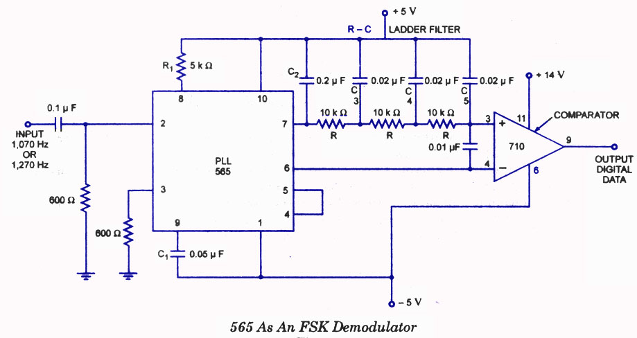
FSK Demodulator
What are Phase-Locked Loops (PLL)? Definition, Block Diagram, Working ... Block Diagram and Working of Phase-Locked Loop The figure here represents the basic block diagram of a phase-locked loop circuit: Let us now move further and understand how each block inside a PLL circuit operates in order to eliminate the phase error between two signals. Phase Detector A phase detector is nothing but a comparator here.

ASOKA TECHNOLOGIES : Design and Simulation of Three Phase Inverter for grid connected ...
Phase-Locked Loop (PLL) Fundamentals | Analog Devices In its most basic configuration, a phase-locked loop compares the phase of a reference signal (F REF) to the phase of an adjustable feedback signal (RF IN) F 0, as seen in Figure 1. In Figure 2 there is a negative feedback control loop operating in the frequency domain.
![2: Complete block diagram of PLL control scheme [30]. | Download Scientific Diagram](https://www.researchgate.net/profile/Md_Amin8/publication/324173825/figure/download/fig3/AS:611395095760902@1522779358398/Complete-block-diagram-of-PLL-control-scheme-30.png)
2: Complete block diagram of PLL control scheme [30]. | Download Scientific Diagram
› lit › anCD4046B Phase-Locked Loop: A Versatile Building Block for ... 4 CD4046B Phase-Locked Loop: A Versatile Building Block for Micropower Digital and Analog Applications 3 CD4046B PLL Technical Description Figure 2 shows a block diagram of the CD4046B, which has been implemented on a single monolithic integrated circuit. The PLL structure consists of a low-power, linear VCO and two
Phase Lock Loop Block Diagram - Wiring Diagram
PDF Phase Locked Loop Circuits - UC Santa Barbara which the loop will lock when starting from an unlocked condition. Sometimes a frequency detector is added to the phase detector to assist in initial acquisition of lock. You will see later that the loop filter bandwidth has an effect on the capture range. 7. Approach: We will discuss the details of phase detectors and loop filters as we proceed.

RAYmaps
› ~jph7 › websiteLock - in Amplifier and Applications - Lehigh University frequency, and θsig is the signal’s phase. Lock-in amplifiers generate their own internal reference signal usually by a phase-locked-loop locked to the external reference. In the diagram below the external reference, the lock-in’s reference and the signal are all shown. The internal reference is VLsin(ωot + θref).
What is the function of PLL(Phase-Locked Loop), and how does work it? - Quora

Constructed Phase Lock Loop - ELEC/595/Burak

Phase Locked Loop Block Diagram - General Wiring Diagram

Phase Locked Loop System Working and Applications

Phase Lock Loop Design and Construction - witchrisriccardi
0 Response to "38 phase lock loop block diagram"
Post a Comment