40 pn junction energy band diagram
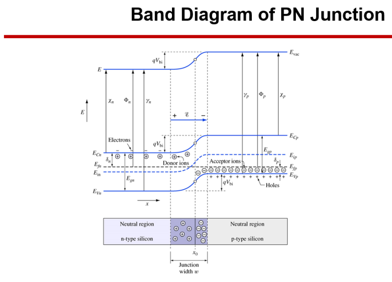
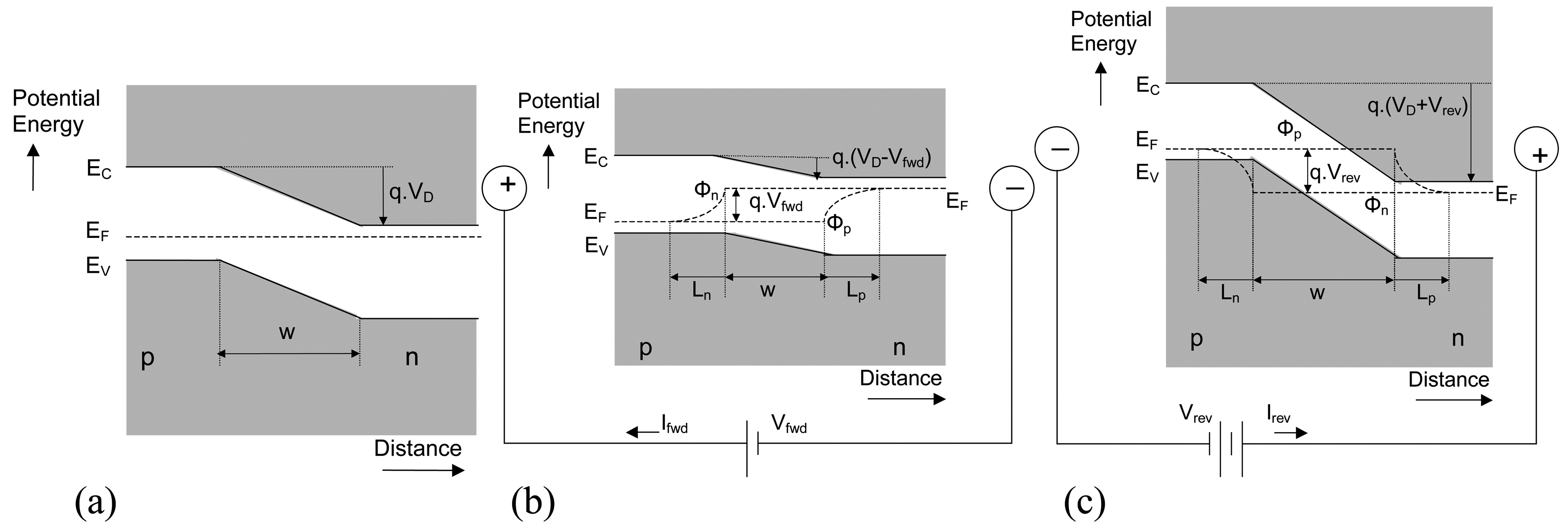
The total potential across the semiconductor equals the built-in the applied E qKI voltage, or:' Energy band diagram of a p-n junction under reverse and forward bias pn-juntion-Diode 15 Electrostatic analysis of a p-n diode The electrostatic analysis of a p-n diode is of interest since it provides knowledge about the charge density and the ... Answer: 4.2. Structure and principle of operation 4.2.1Structure 4.2.2Thermal Equilibrium 4.2.3.The built-In potential 4.2.4The forward and reverse bias A p-n junction consists of two semiconductor regions with opposite doping type as shown in Figure 4.2.1. The region on the left is p-type w...
2.2 A pn Heterojunction Diode Consider a junction of a p-doped semiconductor (semiconductor 1) with an n-doped semiconductor ... of a semiconductor is the energy required to move an electron from the conduction band bottom to the vacuum level and is a material constant. The electron affinity rule ... From the band diagram, one can see that the ...
Pn junction energy band diagram
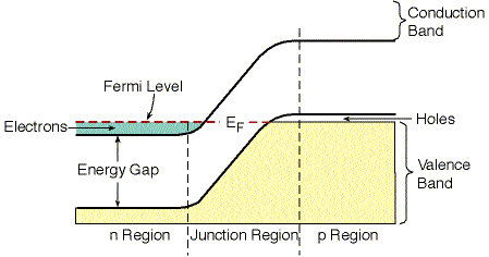
For a p-n junction at equilibrium, the fermi levels match on the two sides of the junctions. Electrons and holes reach an equilibrium at the junction and form a depletion region.The upward direction in the diagram represents increasing electron energy. That implies that you would have to supply energy to get an electron to go up on the diagram, and supply energy to get a hole to go down. The P-N Junction (The Diode). Today: 1. Joining p-and n-doped semiconductors. ... c is the change in the energy of the conduction band across the junction. ... is called a p-n diode and is denoted in circuit diagrams as a following symbol: The current voltage (IV) characteristic for the diode is rectifying and is very different from that ... 1. Diode in the Dark: Construct energy band diagram of . pn-junction. 2. Diode under illumination: Construct energy band diagram. Denote drift, diffusion, and illumination currents. 3. In class exercise: Measure illuminated IV curves. 4. Define parameters that determine solar cell efficiency: • Built-in voltage (V. bi) • Bias voltage (V. bias)
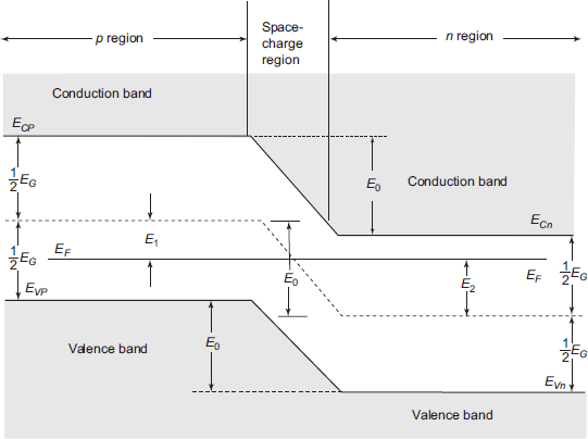
Pn junction energy band diagram. Comparing energy band diagram for metals, semiconductors and insulators 0 In a PN diode, does current flow between the conductors attached to the P and N types valence bands as well as their conduction bands? Energy Band Diagram of P-N Junction Diode. Energy bands are affected based on the biasing techniques applied. The Fermi levels vary when the diode is unbiased as well as it is forward biased or reverse biased. Energy Band of Unbiased Diode. When the diode is unbiased the state of the junction will be at equilibrium. Where, E 0 is the zero bias junction voltage; V T is the thermal voltage of 26mV at room temperature; N D and N A are the impurity concentrations; n i is the intrinsic concentration.; How does current flow in PN junction diode? The flow of electrons from the n-side towards the p-side of the junction takes place when there is an increase in the voltage. A p/n junction is formed when two types of semiconductors, n- type (excess electrons) and p- type (excess holes), come into contact. The term p/n junction refers to the joint interface and the immediate surrounding area of the two semiconductors. The term band gap refers to the energy difference between the top of the valence (outer electron) band and the bottom of the conduction (free ...
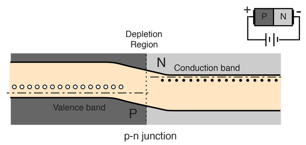
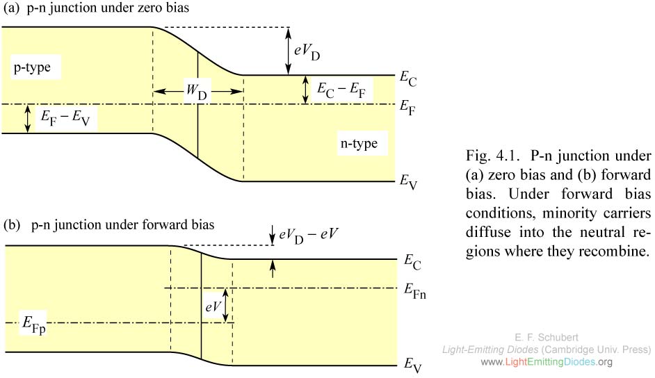
The Forward-Biased p-n Junction If a positive voltage is applied to the p-electrode relative to the n-electrode, the total variation of the electric potential across the junction will decrease. (from Kittel) ... Energy band diagrams showing the intrinsic Fermi level ... Figure 2: Energy band diagram of pand ntype Si before the junction is formed. The location of the Fermi level is di erent for the two semiconduc-tors. Adapted from Principles of Electronic Materials - S.O. Kasap. 2 Contact potential Consider a junction between ptype and ntype Si. The band diagrams In this lecture, i discussed about the energy band diagram of the pn- junction in equilibrium. 8.13 Energy band diagram of p-n diode. The band diagram of isolated p-type and n-type materials are shown in Figs. 8.18 (a) and (b) The Fermi level lies close to the conduction band in n-type material and it is close to valence band in p-type material. When a p-n diode is made with p-type and n-type materials, then flow of free charge carriers ...
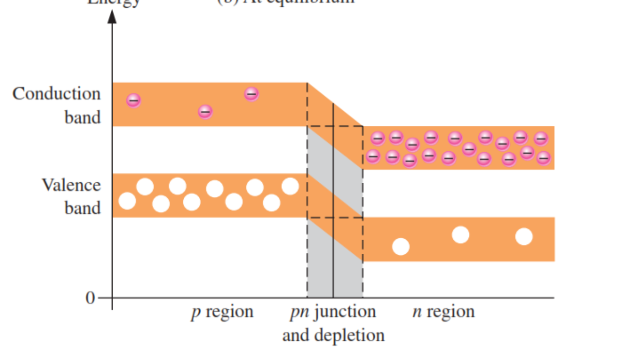
An energy diagram for a pn junction at the instant of formation is shown in Figure (a). As you can see, the valence and conduction bands in the n region are at lower energy levels than those in the p region, but there is a significant amount of overlapping. The free electrons in the n region that occupy the upper part of the conduction band in ... Energy band diagram of a p-n junction in thermal equilibrium While in thermal equilibrium no external voltage is applied between the n-type and p-type material, there is an internal potential, f, which is caused by the workfunction difference between the n-type and p-type pn-juntion-Diode. https://www.patreon.com/edmundsjIf you want to see more of these videos, or would like to say thanks for this one, the best way you can do that is by becomin... Quasi-Fermi levels: Band edge diagram zWhen we draw a band edge diagram out of equilibrium, we need to draw a different Fermi level (quasi-Fermi level) for the electrons and holes zThis, for example, is what the band edge diagram would look like for a forward biased PN diode Quasi Fermi level for electrons Quasi Fermi level for holes} Exactly ...
Download scientific diagram | p-n junction with reversed bias. Energy band diagram is also shown. from publication: Silicon Photo Multipliers Detectors Operating in Geiger Regime: an Unlimited ...

\$\begingroup\$ The Fermi level is a measure of the electron energy. If it was higher or lower some where then electrons would move from the high energy spot to the lower one.. and that motion would then continue till the fermi level was the same everywhere. It's a bit like water seeking the lowest level in a bowl.

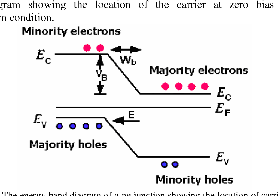
In a p on n structure, this can be accomplished by inserting an electron-blocking unipolar barrier at the junction of the pn diode to form the pBn diode (Klipstein, 2008). Figure 1.12 shows the reverse bias energy band diagrams of a pn diode and a pBn diode, calculated using heterojunction drift-diffusion simulation (Daniel et al., 2000).
P-N Junction One of the crucial keys to solid state electronics is the nature of the P-N junction. When p-type and n-type materials are placed in contact with each other, the junction behaves very differently than either type of material alone. Specifically, current will flow readily in one direction (forward biased) but not in the other (reverse biased), creating the basic diode.

Reverse Biased p-n junction ... approximately parabolic in energy near the conduction and valence band edges (i.e. the DOS goes with the square root of the energy distance above ... For arbitrary charge distributions, band diagrams, junction types, the equationsmay be solved using numerical approaches, and many
Simplified energy band diagram of a p-n junction (a) at equilibrium and (b) under forward bias voltage V. Symbols: E g is the band gap energy of the semiconductor and qV b is the potential barrier ...
The potential energy of an electron is thus higher on the left side of the junction than the right. That is what is plotted on the graph. An electron at the top of the valence band on the the left side will have more energy than one on the right hand side.
Band Diagram xn xp Invert to go from potential to energy scale In equilibrium Fermi-level must be flat Klimeck -ECE606 Fall 2012 -notes adopted from Alam Outline 14 1) Introduction to p-n junctions 2) Drawing band-diagrams 3) Analytical solution in equilibrium 4) Band-diagram with applied bias

1 This idealized PN junction is known as a step junction or an abrupt junction. 4.1.1 Energy Band Diagram and Depletion Layer of a PN Junction Let us construct a rough energy band diagram for a PN junction at equilibrium or zero bias voltage. We first draw a horizontal line for EF in Fig. 4-3a because there is
In solid-state physics of semiconductors, a band diagram is a diagram plotting various key electron energy levels (Fermi level and nearby energy band edges) as a function of some spatial dimension, which is often denoted x. These diagrams help to explain the operation of many kinds of semiconductor devices and to visualize how bands change with position (band bending).
Energy band diagram of a p-n junction (a) before and (b) after merging the n-type and p-type regions Note that this does not automatically align the Fermi energies, E F,n and E F,p . Also, note that this flatband diagram is not an equilibrium diagram since both electrons and holes can lower their energy by crossing the junction.

1. Diode in the Dark: Construct energy band diagram of . pn-junction. 2. Diode under illumination: Construct energy band diagram. Denote drift, diffusion, and illumination currents. 3. In class exercise: Measure illuminated IV curves. 4. Define parameters that determine solar cell efficiency: • Built-in voltage (V. bi) • Bias voltage (V. bias)
The P-N Junction (The Diode). Today: 1. Joining p-and n-doped semiconductors. ... c is the change in the energy of the conduction band across the junction. ... is called a p-n diode and is denoted in circuit diagrams as a following symbol: The current voltage (IV) characteristic for the diode is rectifying and is very different from that ...
For a p-n junction at equilibrium, the fermi levels match on the two sides of the junctions. Electrons and holes reach an equilibrium at the junction and form a depletion region.The upward direction in the diagram represents increasing electron energy. That implies that you would have to supply energy to get an electron to go up on the diagram, and supply energy to get a hole to go down.


0 Response to "40 pn junction energy band diagram"
Post a Comment