42 scanning electron microscope diagram
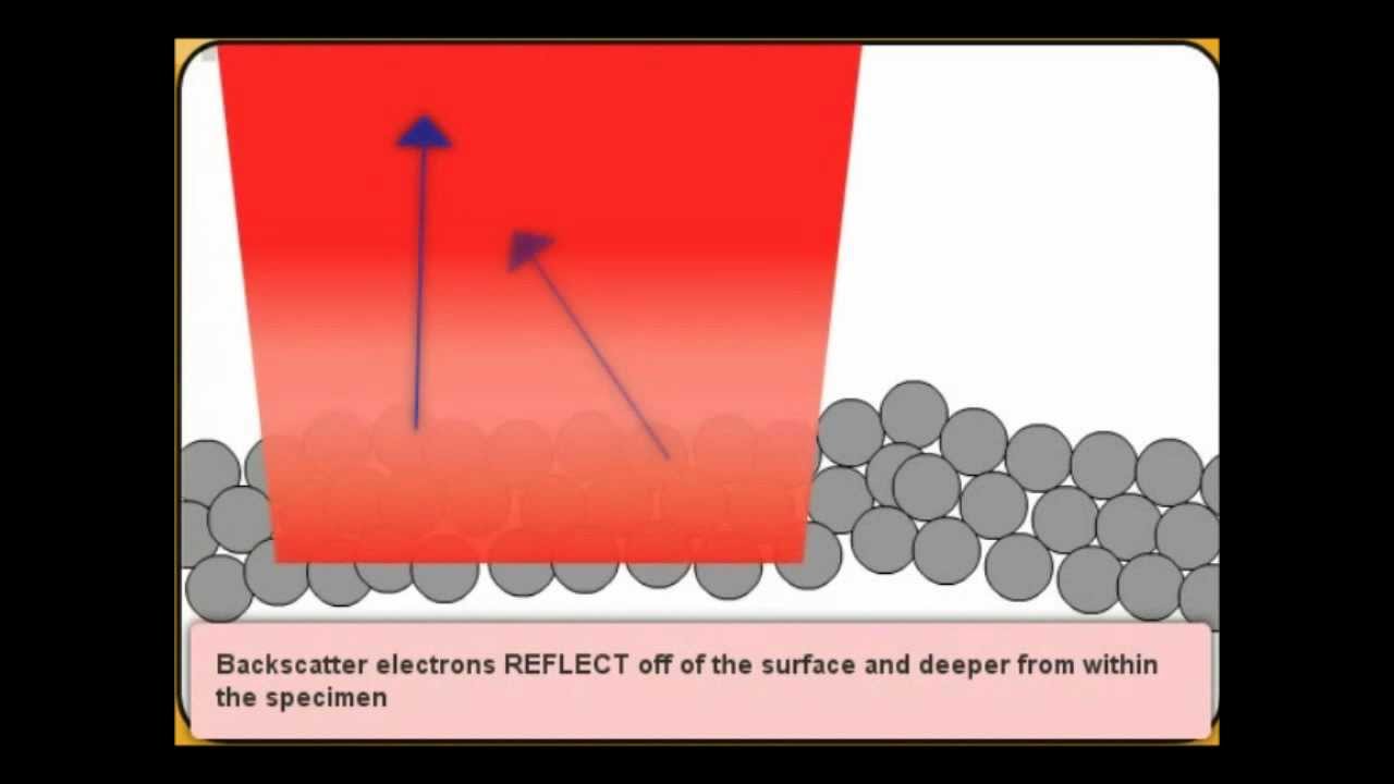
PDF 1 Fundamentals of Scanning Electron Microscopy A close-packed opal structure observed by a field emission scanning electron microscope (FESEM) at different accelerating voltages is shown in Fig. 1.4. Images taken under 1 kV gave more surface details than that of 20 kV. The surface resolution is lost at high accelerating voltages and the surface of spheres looks smooth. 1.1.2. Scanning Electron Microscopy | Materials Science | NREL Scanning Electron Microscopy. In basic scanning electron microscopy (SEM), a beam of highly energetic (0.1-50 keV) electrons is focused on a sample surface. This can produce several interactions including the emission of secondary electrons, backscattered electrons, photons, and X-rays; excitation of phonons; and diffraction under specific ...
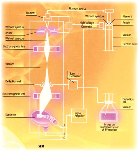
PDF Introduction to Scanning Electron Microscopy Below is a diagram of the electron column and a description of each of the components of the electron column. Figure 2. Scanning electron microscope column [1]. 1) Electron gun: Located at the top of the column where free electrons are generated by thermionic emission from a tungsten filament at ~2700K.

Scanning electron microscope diagram
schematic diagram of scanning electron microscope (SEM ... Scanning Electron Microscope (SEM) images have been recorded in order to understand the morphology of the particles of SnO2 at the nanoscale level. In addition, FT-IR spectra have been obtained to... PDF Scanning Electron Microscopy in Gemology - GIA GIA's scanning electron microscope-energy dispersive spectrometer system. Figure 2. Diagrams of typical electron orbitals, one cut away to show the nucleus. Note that if the nucleus were shown to proper scale with respect to the size of the orbital, it would be invisible in this drawing. Scanning Electron Microscope - an overview | ScienceDirect ... Scanning electron microscope (SEM) images were recorded to obtain the coverage and dispersion of rGO flakes on the interdigitated electrodes after the reduction. Four different GO concentrations were prepared and drop cast onto the electrodes. The corresponding SEM images are shown in Fig. 9. Sign in to download hi-res image Fig. 9.
Scanning electron microscope diagram. Intoduction to Network Structure - Scanning Electron ... Intoduction to Network Structure - Scanning Electron Microscope Manuscript Generator Search Engine. Manuscript Generator Sentences Filter. Translation. English-简体中文. English-繁體中文. English-한국어. English-日本語. English. Introduction to Network Structure - Scanning Electron Microscope ... Scanning Electron Microscopy (SEM) - Methods What is Scanning Electron Microscopy (SEM) A typical SEM instrument, showing the electron column, sample chamber, EDS detector, electronics console, and visual display monitors. The scanning electron microscope (SEM) uses a focused beam of high-energy electrons to generate a variety of signals at the surface of solid specimens. PDF Scanning Electron Microscopy Working Principle An SEM is a type of electron microscope that uses an electron beam to scan the sample. The electrons that are backscattered, as well as the ones that are knocked off the near-surface region of the object, are detected and used to create high-resolution images. How does it work? Applications of Scanning Electron Microscopy Using ... Scanning electron microscopy (SEM) has contributed to elucidating the ultrastructure of bio-specimens in three dimensions. SEM imagery detects several kinds of signals, of which secondary electrons (SEs) and backscattered electrons (BSEs) are the main electrons used in biological and biomedical research.
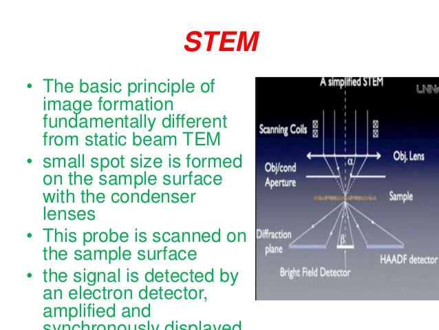
Working Principle of a Electron Microscopes (with Diagram) In a scanning electron microscope, the specimen is exposed to a narrow electron beam from an electron gun, which rapidly moves over or scans the surface of the specimen (Figure 4.13). This causes the release of a shower of secondary electrons and other types of radiations from the specimen surface. PDF Scanning Electron Microscope - Yola The electron beam is generally scanned in a raster scan pattern, and the beam's position is combined with the detected signal to produce an image. The electron beam can focused to a spot approximately 1 nanometer in diameter, and microscopes are able to resolve details ranging from 1-20 nm in size. PPT PowerPoint Presentation Do it with electrons ! SEM - scanning electron microscopy Resolution Determined by probe size SEM - scanning electron microscopy Depth of field d = depth of field = required spatial resolution a = convergence angle d region of image in focus For small angles, tana = a Can control depth of field (d) with convergence angle (a) SEM - scanning electron microscopy Depth of field WD Rap * Microscopy ... Scanning Electron Microscope - Radiological and ... A beam of electrons is produced at the top of the microscope by an electron gun. The electron beam follows a vertical path through the microscope, which is held within a vacuum. The beam travels through electromagnetic fields and lenses, which focus the beam down toward the sample.
Scanning Electron Microscopy - an overview | ScienceDirect ... Scanning electron microscopy Figure 29.6. The flakes are 50-100 μm in diameter. SEM can also be used to examine the consolidated resin, as shown in Figure 29.7.This sample was freeze-fractured by immersing in liquid nitrogen for 1 h, then striking rapidly with a dull blade at a prescored mark [4], and clearly shows the UHMWPE flakes on the freeze-fractured surface. Scanning Electron Microscope (SEM)- Definition, Principle ... Scanning Electron Microscope (SEM) Definition. Scanning Electron Microscope (SEM) is a type of electron microscope that scans surfaces of microorganisms that uses a beam of electrons moving at low energy to focus and scan specimens. The development of electron microscopes was due to the inefficiency of the wavelength of light microscopes. electron microscopes have very short wavelengths in ... Scanning Electron Microscopy (SEM) - Techniques What is Scanning Electron Microscopy (SEM) A typical SEM instrument, showing the electron column, sample chamber, EDS detector, electronics console, and visual display monitors. The scanning electron microscope (SEM) uses a focused beam of high-energy electrons to generate a variety of signals at the surface of solid specimens. Scanning electron microscope - Wikipedia A scanning electron microscope ( SEM) is a type of electron microscope that produces images of a sample by scanning the surface with a focused beam of electrons. The electrons interact with atoms in the sample, producing various signals that contain information about the surface topography and composition of the sample.
Patent US6646262 - Scanning electron microscope - Google Patents
Scanning Electron Microscopy Scanning Electron Microscopy Volume 1986 Number 4 Article 18 10-9-1986 Cryoultramicrotomy and Immunocytochemistry in the Analysis of Muscle Fine Structure L. -E. Thornell University of Umeå G. S. Butler-Browne Institut Pasteur E. Carlsson University of Umeå H. M. Eppenberger Swiss Federal Institute of Technology D. O. Fürst

SCANNING ELECTRON MICROSCOPE - YouTube
Scanning electron microscopy - LNF Wiki Scanning electron microscopy (SEM) is one of the most versatile instruments available for the examination and analysis of the microstructure morphology and chemical composition characterizations. This examination can yield information about the topography (surface features of an object), morphology (shape and size of the particles making up the object), composition (the elements and compounds ...
| Scanning electron microscopy (SEM) and transmission electron... | Download Scientific Diagram
Scanning Electron Microscope Service Scanning electron microscope (SEM) is an observation method. It does not use electromagnetic lens to amplify the image but uses a narrow focused-high-energy electron beam to scan the sample, which in a similar way of television photography. SEM stimulates various physical information through the interaction between the beam and the material ...
Figure 1: Scanning electron microscopy images of potato and apple parenchyma. | Scientific Diagram
Scanning electron microscopy of nuclear structure This is due to the overall size and largely fibrous nature of the contents, making large scale 3D reconstructions difficult from thin sections using transmission electron microscopy. This chapter brings together a number of methods developed for visualization of nuclear structure by scanning electron microscopy (SEM).
Scanning transmission electron microscope
(PDF) Scanning Electrochemical Microscopy. 59. Effect of ... Scanning electron microscopy (SEM) of with physisorbed methylene blue (MB) concluded that the ET electrodeposited Pd nanoparticles provides independent evidence for MB reduction was predominantly through pinholes.20,21 of the presence of pinholes on a SAM.

Electron Microscope Images Images, Stock Photos & Vectors | Shutterstock
Scanning Electron Microscope (SEM) - Diagram, Working ... Scanning electron microscope is a classification of electron microscope that uses raster scanning to produce the images of a specimen by scanning using a focused electron beam on the surface of the specimen. An SEM creates magnified images of the specimen by probing along a rectangular area of the specimen with a focused electron beam.
How a Scanning Electron Microscope Works.wmv - YouTube
With a neat diagram explain construction and working of ... these collected electrons produce scintillations on to the photo multiplier tube are converted into electrical signals. these signals are amplified by the video amplifier and is fed to the CRO. By similar procedure the electron beam scans from left to right and the whole picture of the sample is obtained in the screen.

Scanning Electron Microscope Blog: Fungi - Images for Eastfield College Microbiology
Scanning electron microscope (SEM): Structure and ... A scanning electron microscope (SEM) is a type of powerful electron microscope where objects are observed using fast-moving electron particles. This microscope observes a variety of organic and inorganic substances from 1 nanometer to micrometer. In 1937 Manfred Von Ardenne first invented the scanning electron microscope.
A scanning electron microscope | sonic wallpaper
Schematic diagram of Scanning Electron Microscope ... Scanning Electron Microscope (SEM) is a powerful magnification tool that utilizes focused beams of electrons to obtain information. The high-resolution, three dimensional images produced by SEMs...
0 Response to "42 scanning electron microscope diagram"
Post a Comment