39 schottky diode band diagram
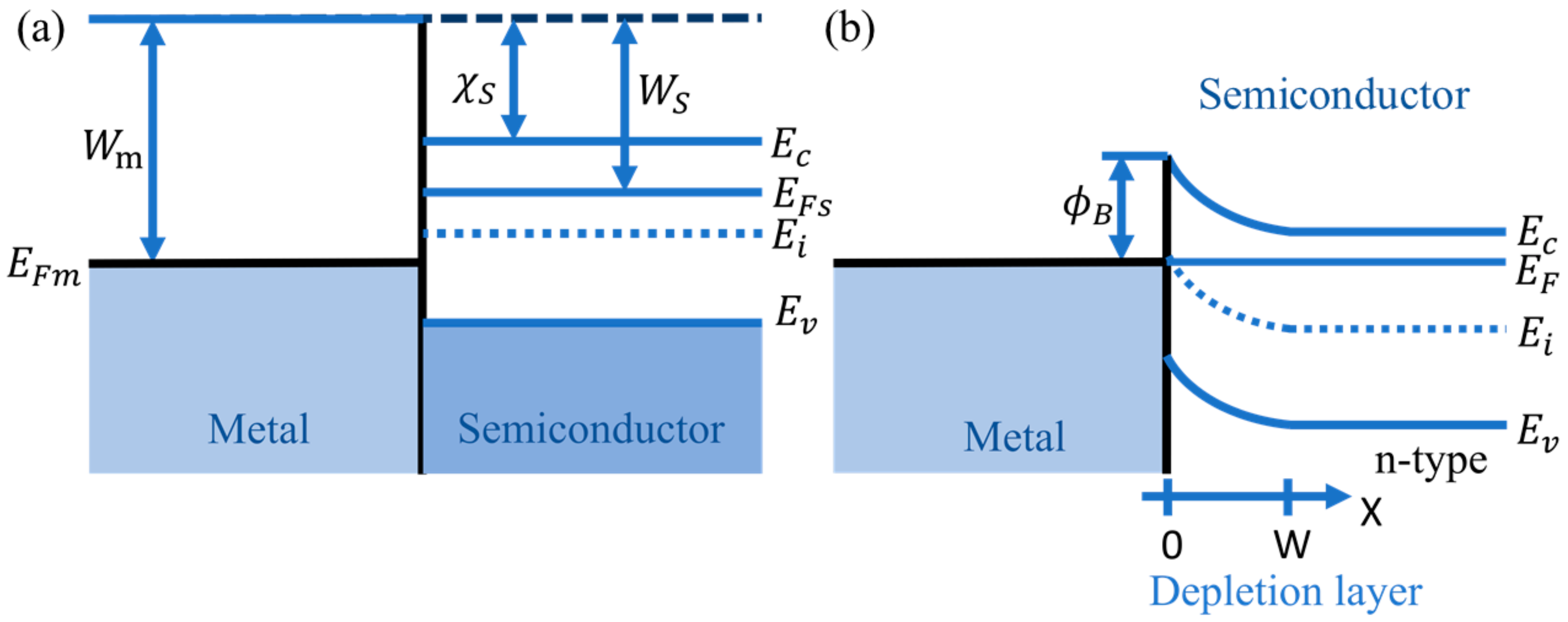
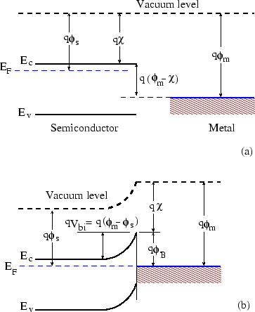
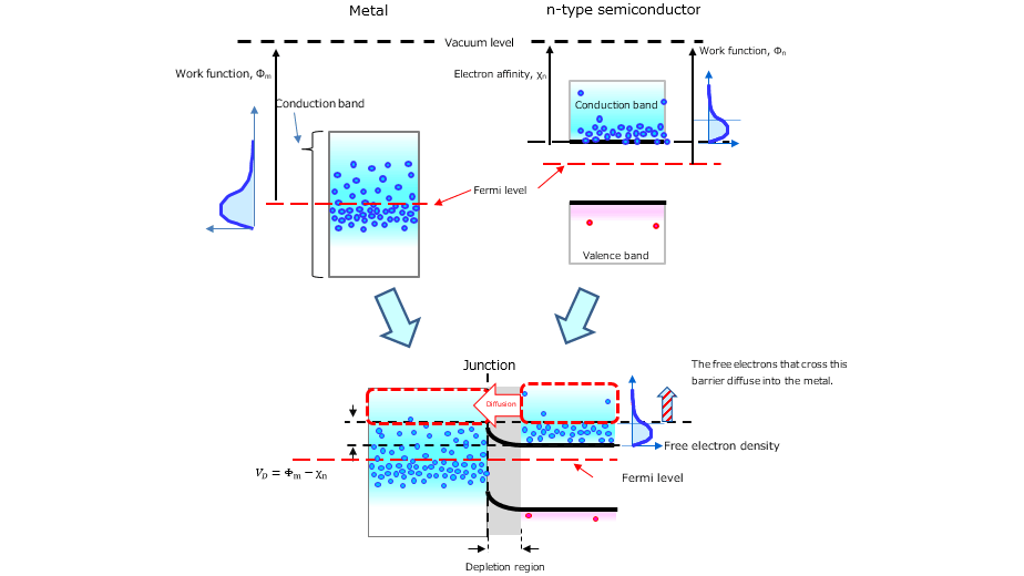
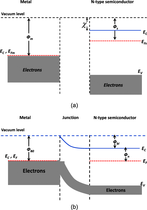
Band bending - Wikipedia Metal-semiconductor contact induced band bending. Figure 1 shows the ideal band diagram (i.e. the band diagram at zero temperature without any impurities, defects or contaminants) of a metal with an n-type semiconductor before (top) and after contact (bottom). The work function is defined as the energy difference between the Fermi level of the material and the vacuum level before … Stretchable rubber diode opens possibilities for medical, … Dec 01, 2022 · (E) An optical microscopic image of the diode. (F) I-V characteristics of the rubbery Schottky diode under the mechanical strain of 0, 10, 20, and 30%. (G) Energy levels of AgNWs, AuNPs, P3HT-NFs, and liquid metal. (H) Illustration of the energy band diagram of the metal (liquid metal)– and p-type semiconductor (P3HT)–based Schottky junction.
(a) Energy band diagram of the Schottky photodetector. (b) Schematic of ... Simulations show that for the proposed photodetector with 2-nm-thick Au, Cu, and Ag Schottky contacts, the absorptance dramatically enhances to 95.1%, 93.2%, and 98.2%, respectively, at the ...
Schottky diode band diagram
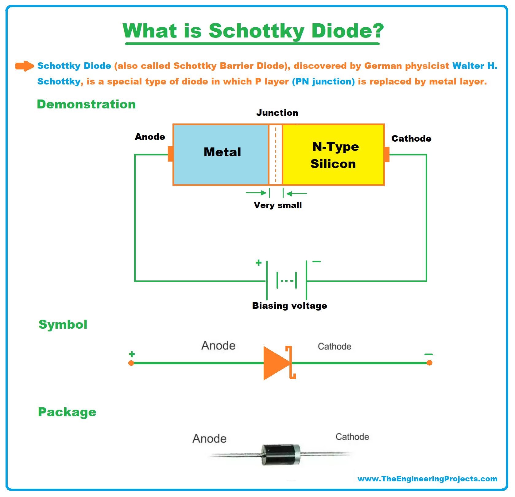
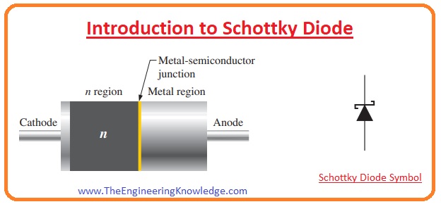
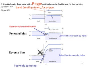
Schottky diode - Definition, Symbol, Working and Applications - Diode Energy band diagram of schottky diode The energy band diagram of the N-type semiconductor and metal is shown in the below figure. The vacuum level is defined as the energy level of electrons that are outside the material. The work function is defined as the energy required to move an electron from Fermi level (EF) to vacuum level (E0). Schottky Diode - Definition, Symbol, VI Characteristics, Applications The schottky diode is a type of metal - semiconductor junction diode, which is also known as hot-carrier diode, low voltage diode or schottky barrier diode. The schottky diode is formed by the junction of a semiconductor with a metal. Schottky diode offers fast switching action and has a low forward voltage drop. Energy band diagram of a metal-semiconductor Schottky diode with a p ... Energy band diagram of a metal-semiconductor Schottky diode with a p -doped quantum well, ͑ a ͒ without bias and ͑ b ͒ with forward bias. E c Source publication Near-infrared to visible...
Schottky diode band diagram. The energy band diagram for Al/Gelatin/n-Si Schottky diode. Download scientific diagram | The energy band diagram for Al/Gelatin/n-Si Schottky diode. from publication: Investigation of Trap States, Series Resistance and Diode Parameters in Al/Gelatin/n-Si ... Metal-Semiconductors Contacts - Engineering LibreTexts Figure 1 shows the energy band diagram after the contact is made. As shown in Figure 1, the vacuum level E0, the minimum energy needed to release an electron from the material, is used to align the metal and the semiconductor together. The work function Φ is defined as the energy difference between the Fermi energy and the vacuum level. A Review on Conduction Mechanisms in Dielectric Films - Hindawi Thermionic-field emission takes place intermediately between field emission and Schottky emission. In this condition, the tunneling electrons should have the energy between the Fermi level of metal and the conduction band edge of dielectric. The schematic energy band diagram of thermionic-field emission is shown in Figure 10(a). PDF Schottky diode - TU Graz Schottky diode Draw the band diagram (valence band, conduction band, Fermi energy) for a Schottky diode with a n doped semiconductor and a p doped semiconductor at zero bias. Assume that interface states pin the Fermi energy to the middle of the semiconducting gap at the interface.
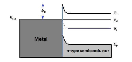
Schottky diode - Wikipedia The Schottky diode (named after the German physicist Walter H. Schottky ), also known as Schottky barrier diode or hot-carrier diode, is a semiconductor diode formed by the junction of a semiconductor with a metal. It has a low forward voltage drop and a very fast switching action. Schottky diode and its band diagram - YouTube Hi,this video teaches about Schottky diode ,its energy band diagram,question and important formula's.learn by questionLearn By Questionlearnbyquestionformula... Schottky Diode Part 1 - Band Diagram - YouTube Schottky Diode Part 1 - Band Diagram 37,681 views May 16, 2019 576 Dislike Share Jordan Edmunds 36.7K subscribers If you want to see more of these videos,... PDF Chapter 9 Metal-Semiconductor Contacts - University of California, Berkeley 9.1 Schottky Barriers Energy Band Diagram of Schottky Contact • Schottky barrier height, φB, is a function of the metal material. • φB is the single most important parameter. The sum of qφBn and qφBp is equal to Eg. Metal Depletion layer Neutral region qφBn Ec Ec Ef Ef Ev qφ Ev Bp
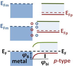
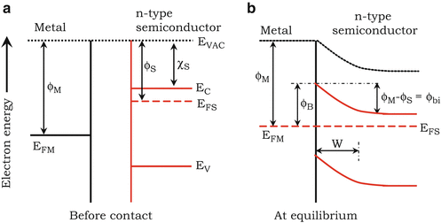
Band diagram - Wikipedia Band diagram for Schottky barrier at equilibrium Band diagram for semiconductor heterojunction at equilibrium In solid-state physics of semiconductors, a band diagram is a diagram plotting various key electron energy levels ( Fermi level and nearby energy band edges) as a function of some spatial dimension, which is often denoted x. [1] Band diagram and capacitance of a Schottky diode 3.1.2 Band diagram and capacitance of a Schottky diode. Then, using Eq. (3.12), the ac component of the occupation function is given by: ) cnndc >>e p (we neglect exchanges with the valence band), and Eq. (3.13) reduces to: The capacitance C being related to the response of gap states to the small ac bias signal, it can be observed in Eq. (3.14 ... Solved Draw the equilibrium band diagram of a p-type | Chegg.com Draw the equilibrium band diagram of a p-type Schottky diode with the following information: The metal work function is 5 eV The ionization potential of Si is 5.6 eV The work function of silicon is 5.5 eV Determine the barrier height and built in potential of the Schottky diode. s.pdf - Schottky diode Draw the band diagram (valence band,... Schottky diode Draw the band diagram (valence band, conduction band, Fermi energy) for a Schottky diode with a n doped semiconductor and a p doped semiconductor at zero bias. Assume that interface states pin the Fermi energy to the middle of the semiconducting gap at the interface. Indicate where the depletion region is and explain why it is depleted. ...
Electrical Properties of a Ga In N As p-i-n Schottky Barrier ...
Schottky barrier - Wikipedia A Schottky barrier, named after Walter H. Schottky, is a potential energy barrier for electrons formed at a metal–semiconductor junction.Schottky barriers have rectifying characteristics, suitable for use as a diode.One of the primary characteristics of a Schottky barrier is the Schottky barrier height, denoted by Φ B (see figure). The value of Φ B depends on the …

Best Tutorial on Schottky Diode - EeeStudy
Band diagram of CIS NW - Al Schottky diode - 1library.net Figure 6.5: .Sketch of the energy band diagram of a CIS-Al Schottky diode. To construct this diagram, the electron affinity values were taken to be 4.48 eV for where, N V is the effective density of states in the valance band of CIS; k is Boltzman‟s constant; h is Planck‟s constant and T is temperature.
Schottky Diode: Definition, Working & Characteristics - The ...
Everything You Need To Know About Schottky Diode - ICRFQ The diagram below presents a Schottky diode's V-I (Voltage-Current) properties. The vertical line in the diagram below shows the current flow through the Schottky diode, while horizontal line is what represents the voltage present across a Schottky diode. Schottky diodes have V-I properties that are almost identical to P-N junction diodes.
Micromachines | Free Full-Text | Electrical Characterizations ...
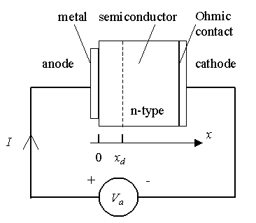
Ohmic Contacts, Schottky Barriers and Schottky Diodes The formation of a Schottky diode is illustrated in Figure 2.25b, in which negative charge is trapped at the junction. The Schottky diode is also referred to as an MS diode or Metal-Semiconductor diode. This diode will now be discussed and modelled.
Introduction to Schottky Diode, Pins, Working, Construction ...
Microwave - Wikipedia Microwave is a form of electromagnetic radiation with wavelengths ranging from about one meter to one millimeter corresponding to frequencies between 300 MHz and 300 GHz respectively. Different sources define different frequency ranges as microwaves; the above broad definition includes both UHF and EHF (millimeter wave) bands.A more common definition in radio …

Schottky Diode Part 1 - Band Diagram
Schottky Diode - NCU Energy band diagram of a silicon Schottky barrier with f B = 0.8 V and N d = 10 19 cm-3. Shown is the energy band diagram obtained using the full-depletion approximation, the potential reduction experienced by electrons, which approach the interface and the resulting conduction band edge. ... In a Schottky diode, the semiconductor band diagram ...
Schottky diode - Citizendium
CMOS - Wikipedia The power supply pins for CMOS are called V DD and V SS, or V CC and Ground(GND) depending on the manufacturer. V DD and V SS are carryovers from conventional MOS circuits and stand for the drain and source supplies. These do not apply directly to CMOS, since both supplies are really source supplies. V CC and Ground are carryovers from TTL logic and that …

Schottky Barrier Diode - Power Microelectronics. Device and ...
Semiconductor Diode: Definition, Types, Characteristics and … Sep 26, 2022 · Diode Under Reverse Bias. Now, when we apply an external voltage across the diode, the sum of total barrier voltage becomes V 0 +V as here the direction of external voltage is in the same direction as the direction of barrier potential. The depletion region’s width increases and hence the motion current carriers that move from one side of the junction to the other one …
Band diagram of a Schottky diode on n-type silicon ...
Diode - Wikipedia A diode is a two-terminal electronic component that conducts current primarily in one direction (asymmetric conductance); it has low (ideally zero) resistance in one direction, and high (ideally infinite) resistance in the other.. A diode vacuum tube or thermionic diode is a vacuum tube with two electrodes, a heated cathode and a plate, in which electrons can flow in only one direction, …
Lecture 4 4521 semiconductor device physics - metal ...
Energy band diagram of a metal-semiconductor Schottky diode with a p ... Energy band diagram of a metal-semiconductor Schottky diode with a p -doped quantum well, ͑ a ͒ without bias and ͑ b ͒ with forward bias. E c Source publication Near-infrared to visible...

Schottky Diode - an overview | ScienceDirect Topics
Schottky Diode - Definition, Symbol, VI Characteristics, Applications The schottky diode is a type of metal - semiconductor junction diode, which is also known as hot-carrier diode, low voltage diode or schottky barrier diode. The schottky diode is formed by the junction of a semiconductor with a metal. Schottky diode offers fast switching action and has a low forward voltage drop.
3.1.6.2 Schottky Contact
Schottky diode - Definition, Symbol, Working and Applications - Diode Energy band diagram of schottky diode The energy band diagram of the N-type semiconductor and metal is shown in the below figure. The vacuum level is defined as the energy level of electrons that are outside the material. The work function is defined as the energy required to move an electron from Fermi level (EF) to vacuum level (E0).
Role of Schottky Barrier Height Modulation on the Reverse ...

Schottky barrier - Wikipedia

Schottky Diode
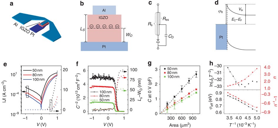
Flexible indium–gallium–zinc–oxide Schottky diode operating ...

Schottky Barrier - an overview | ScienceDirect Topics

Lecture 7 OUTLINE Poisson's equation Work function Metal ...

Schottky diode - Definition, Symbol, Working and Applications ...

Metal–semiconductor junction - Wikipedia

Metal-semiconductor-metal heterojunction diodes consisting of ...
Lecture contents
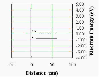
Table of contents
2-1. Schottky contact (Schottky junction) Φm > Φ ...
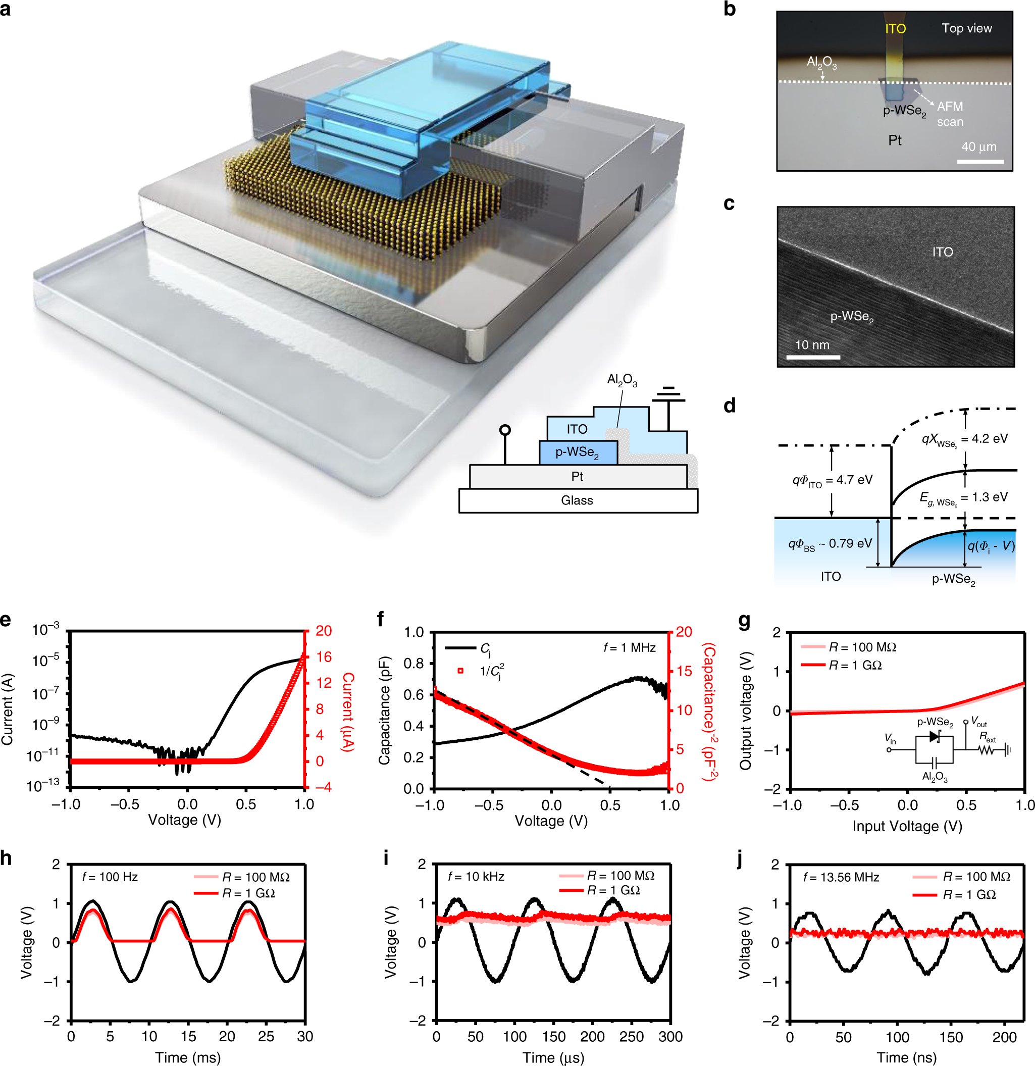
Ultrafast 27 GHz cutoff frequency in vertical WSe2 Schottky ...
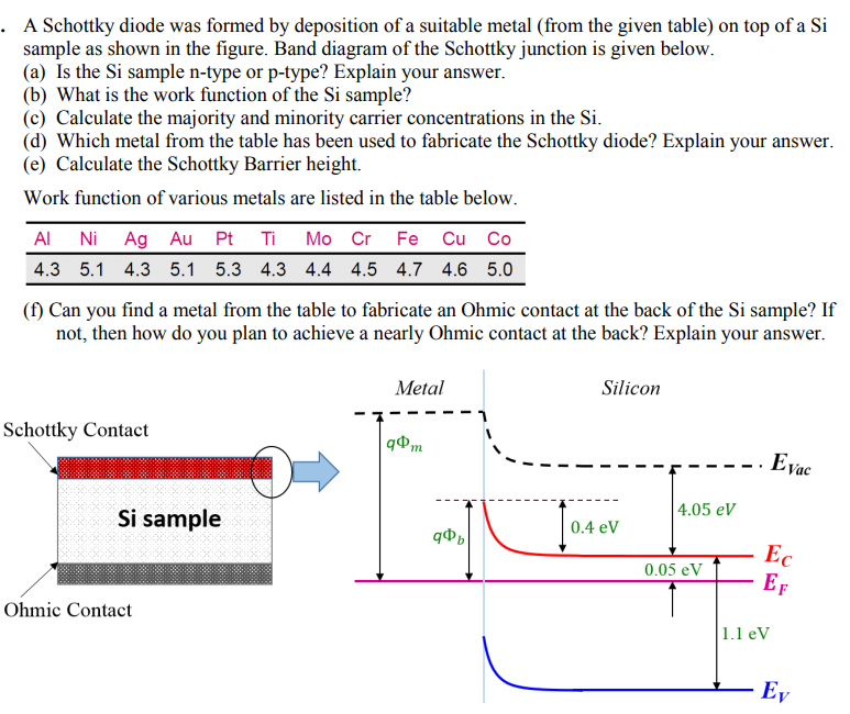
Solved A Schottky diode was formed by deposition of a | Chegg.com
Semiconductor Junctions, Solid-Solid Junctions | SpringerLink
Lecture contents
1 Graphene Schottky diodes: an experimental review of the ...
Lecture 4 4521 semiconductor device physics - metal ...
Near-ideal van der Waals rectifiers based on all-two ...
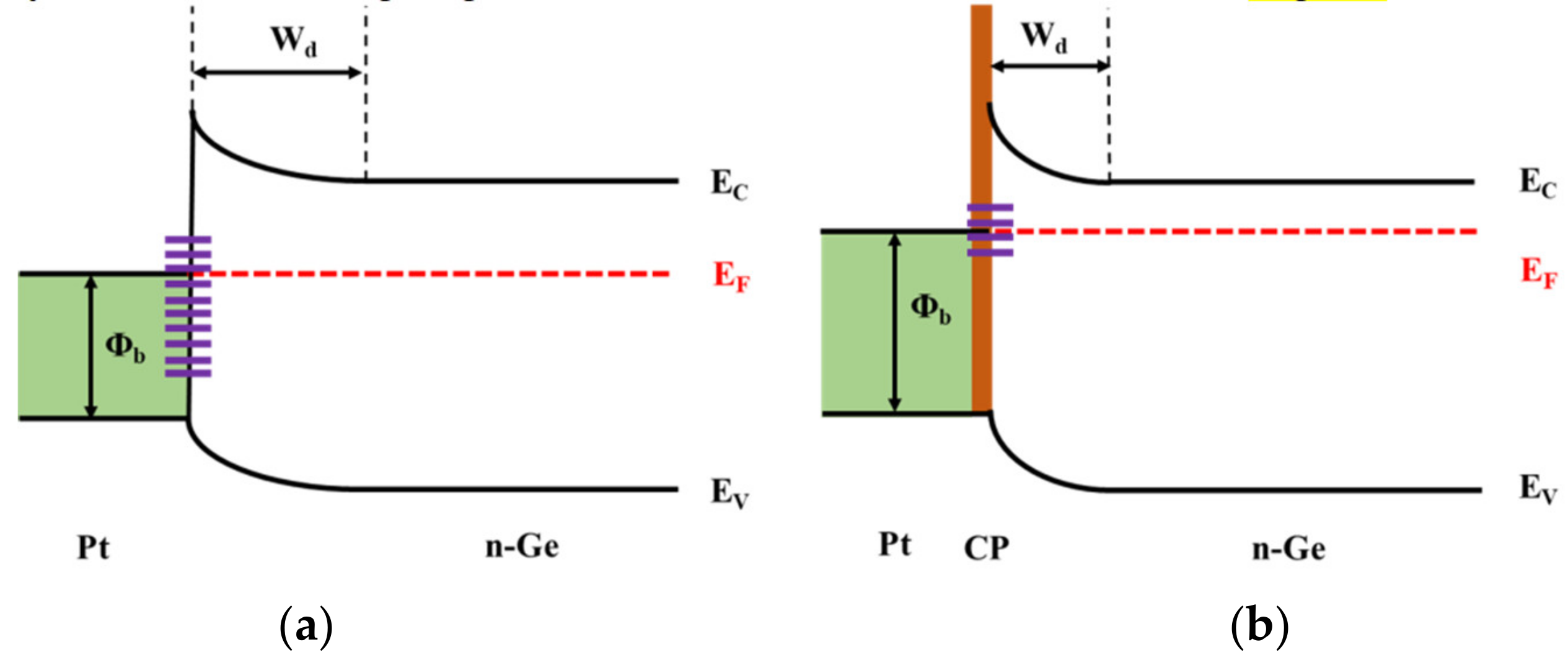
Crystals | Free Full-Text | A Stable and Efficient Pt/n-Type ...
Metal-Semiconductors Contacts - Engineering LibreTexts

Band diagram of the Schottky Junction explaining the sensing ...
1 Graphene Schottky diodes: an experimental review of the ...

The effect of shunt resistance on the electrical ...

SSPD_Chapter 3_Section 3.4.Schottky Diode and Section 3.5 ...
Everything You Need To Know About Schottky Diode
Schottky Diode
0 Response to "39 schottky diode band diagram"
Post a Comment